AI hardware has been a pretty simple game for years: Whose GPU has the most FLOPS, the most memory, or the fastest clock? But as hyperscalers want more performance from the same size of facilities, who controls the fabric between the chips is becoming another question frequently asked – in large part because it can dictate whether AI hardware follows the principles of Moore’s law that have held for decades, or breaks out into a new paradigm.
“Moore's Law is deader than a doornail, absolutely just toast,” said Nick Harris, chief executive of photonics firm Lightmatter, in an interview with Tom's Hardware Premium. The way to make a processor faster used to be to pack in more silicon, but there is a physical limit to how big a single chip can be – so performance now depends on networking dozens, then hundreds, of chips together. “Ultimately, networking is the future of computing,” Harris said. “The performance of these AI systems is completely hamstrung and bottlenecked by your ability to achieve low latency and very, very high bandwidth.”
It all comes down to scale-up and scale-out. Scale-up is the ultra-low-latency interconnect inside a single server, rack, or pod that makes many accelerators behave like one giant machine. Scale-out is the wider network, combining those machines into clusters. There is a third factor, called scale-across, that links whole data centers together. As Polina Bayvel, professor of optical communications and networks at University College London, told us, the hyperscalers are "on a drug which says that the more you put in, the better is the answer" – and between 72 and 144 GPUs now go into a single scale-up rack before it needs to reach outward.
Copper was sufficient within racks for years, but it has hit a wall, and a supply shortage. “Your arm reach, my arm reach, is about two metres – the copper cable is a little shorter than that,” Harris explained, “and we’ve already hit the limit.” Thus, optical interconnects are becoming more important, and moving from rack-to-rack cabling toward the accelerator package itself. Earlier this month, Elon Musk made moves to purchase Mesh Optical, as part of TeraFab and SpaceX's ongoing AI ambitions.
Moving light towards the chip
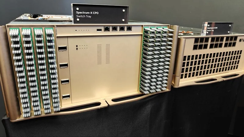
Today, optical signals usually arrive through pluggable transceivers, the standard modules that sit around 18 inches from the switch. The next step is near-package optics, which brings that down to roughly six inches. After that comes co-packaged optics, or CPO, where optical chiplets sit around the GPU or switch. The most ambitious version puts the optics on an interposer beneath the chip itself. “As you progress, you increase the speed and you reduce the energy consumption with each one of those leaps,” said Harris.
For now, the industry’s attention is on the step before the really radical one. “I think 2027 and 2028 are going to be very, very big years for near-package optics,” Harris said. He describes it as the test bed: the last stop before the optical transceiver effectively ships as part of the accelerator or switch, rather than as a separate component bolted on nearby.
Lightmatter is already building CPO parts at TSMC and GlobalFoundries, which it expects to ship in 2028. At the same time, it is working with customers on the more integrated interposer approach – the one for companies that, in Harris’s words, “realise they’d like to have an advantage in the market.”
The reason is power. Bayvel says about 20 percent of a data center’s energy goes into networking: The business of connecting GPUs and CPUs across racks, rooms and data centres. The other 80 per cent is consumed by the GPUs themselves. But she is clear-eyed about what happens to any savings. “Whatever energy you save through optics isn’t going to be there for saving the world,” she said. “It’s to stick another 1,000 GPUs in.”
Warring standards
Nvidia has a vertically integrated answer spanning both domains, from NVLink and NVSwitch for scale-up to Spectrum-X Ethernet and InfiniBand for scale-out. The rest of the industry, including AMD, Broadcom, Cisco, Arista, Marvell, Meta, Microsoft and OpenAI, is trying to prise that open through UALink, Ultra Ethernet and a new optical specification.
The sense that a standards war is building is becoming obvious. At Computex, AMD showed its Helios MI455X platform, a 72-GPU rack meant to rival Nvidia's Vera Rubin NVL72. But its scale-up fabric runs UALink-over-Ethernet rather than native UALink – a stopgap forced by the fact that dedicated UALink switching silicon from partners such as Astera Labs and Marvell was not ready in time. Engineering samples are due in the second half of 2026, with mass production slipping to Q2 2027, while AMD's next-generation MI500-series rack is expected to follow quickly.
Bayvel says the wider contest is one between CPO and linear-drive pluggable optics (LPO). CPO integrates lasers and optics alongside the processing and is probably more power-efficient, “but probably less reliable –so if your laser fails, you need to replace the whole board.” LPO keeps things in conventional pluggable slots and is more serviceable. “There’ll be a brave person who will bet their house on which will win,” she said. She guesses that they coexist, split by application, with a rough 60/40 lean towards CPO.
The laser bottleneck
The problem is that silicon can do almost everything except the one thing this industry increasingly needs it to do: shine.
Silicon is cheap, abundant, and brilliant for electronics. It is why the modern chip industry exists. But it is terrible at emitting light. “Silicon doesn’t emit light at all — that’s a big problem,” said Frederic Gardes, professor of silicon photonics at the University of Southampton, in an interview with Tom’s Hardware Premium.
For decades, the industry has worked around that by using so-called III-V materials such as indium phosphide and gallium arsenide, which are much better at producing light. But that fix brings its own problem. Those materials sit in a much tighter, more geopolitically exposed supply chain, with China controlling around 80 percent of supply. Getting lasers onto silicon is, Gardes said, “one of the key problems” the field now has to solve.
But it’s also where the money is. “Half of the revenue opportunity for this industry is lasers,” Harris said. “It’s a freaking power supply, but it turns out that it’s half of the revenue opportunity.” The irony is that the bit everyone needs most is also the bit that may prove most fragile. Gardes calls lasers “the weakest link.”
That weakness is already showing up in the supply chain. Laser makers Lumentum and Coherent are booked out for years. And the industry is starting to standardise. In March, AMD, Broadcom, Meta, Microsoft, Nvidia and OpenAI founded the Optical Compute Interconnect (OCI) Multi-Source Agreement, a hyperscaler-led effort to define a common optical physical layer for scale-up — one that can carry both NVLink and UALink, starting at 200Gbps per direction and scaling towards 3.2Tbps per fibre.
Whichever route wins, Bayvel worries the industry is fixating on the data center while neglecting the networks that must carry all this AI-generated traffic across land, sea and space. “Really, nobody’s looking at that,” she said, “and I think that's going to be a big problem down the line.”
Chris Stokel-Walker is a Tom's Hardware contributor who focuses on the tech sector and its impact on our daily lives— online and offline. He is the author of How AI Ate the World, published in 2024, as well as TikTok Boom, YouTubers, and The History of the Internet in Byte-Sized Chunks.